
The Photonics Supply Chain
From fundamentals to opportunities, one name at a time

This write up is a complete and comprehensive overview of the photonics sector and opportunity, a complex sector which is supposed to reshape AI datacenters and push their potential even further.
We will start by the need and the technology itself, what it is and why is their a need to upgrade our datacenters, and then go over the entire supply chain to have a global overview of the companies involved in this new technologies, their role in the supply chain and how they interact with each other.
The sector has received lots of liquidity and stocks already returned hundreds of percent, but as this technology could be the next foundation for scaling inference, the opportunity wouldn’t stop after those returns and we should be ready for when (not if) the breathers happen.
The opportunity is clear, the technology is backed by serious capital and people, the speculative part of investing, betting on if the technology will be adopted, is behind us and what lies ahead is scaling - with order books and revenue growth. Analysts have no idea on what to expect and this is when the risk reward will be the best - on the breathers happening after fundamental confirmations but before the first financial ones.
This is what makes the opportunity so interesting today; while it is just starting, while analysts have no idea of what is coming, while most of these companies are still pretty small and ignored by the biggest players.
Late enough to avoid all the risks. Early enough to reap more than enough returns.
Physics & Bottlenecks
Before going over photonics themselves, we need to review some concepts we’ve already seen - like datacenters or GPUs, which I’ll go over again briefly.
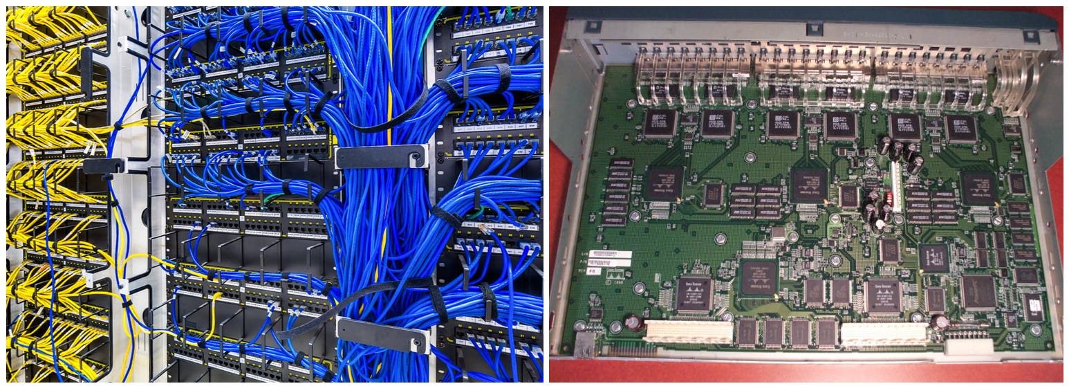
Datacenters are the interconnexion of thousands of hardware, each with its own specialty; a hardware is the interconnexion of hundreds of semiconductors. Data transits through them via electrical or optical “cables” between them in the datacenter or conductive metals - copper as the cheapest conductor to scale, within the hardware.
Artificial Intelligence is this famous new technology, born from data and compute. A model learning from billions of iterations to guess the next token - which could be anything from a letter to a pixel passing by an action, each mistake forcing the model to update its parameters during training by adjusting weights in how the next token is guessed, until reaching satisfaction. AI learns just like you do, by repeating a task and adapting as your mistakes teach you how you should do things, until you get it right - until you are satisfied at least.
For decades, the AI bottleneck was compute, the question being how do we treat so much data, how do we guess the next token fast enough so a simple task like writing a one-line text doesn’t take weeks?
This was resolved by GPUs, semiconductors designed to do parallel computing and behave like a hive. Thousands of GPUs would be allocated to one task, each only working on a fraction of the problem, be fed the required data to solve it and share the result with the hive. This new computing method, GPUs parallel computing instead of CPUs sequential computing, allowed model training with human timeframes.
GPUs are made from specific semiconductors, optimized and small. AI democratized, its potential became very clear and demand for compute rose exponentially, reaching a point where physics were limiting its deployment. This created an entire ecosystem, some would call it a circular economy, with many large winners in the stock market, as you all already know.
Then came inference, the usage of those models. Musicians learn music theory early on, but eventually they need to pick up their instruments. Imagine you have trained all your life and your final exam will be someone - let’s say me, giving you a song. Any song, with the required music sheet, and you’ll need to play it well enough so I’m satisfied. This is inference, the model knows, now it has to be used for what it was trained - whatever it is from driving to generating images.
The issue with inference is, it is limited. The model itself and its capacities aren’t, it could answer perfectly to your needs - assuming it is trained perfectly, just like you will take your guitar and play me Sweet Home Alabama if I give you the music sheet. But imagine if 10M people gave you a different music sheet at the same time and asked you to play them all, simultaneously. You couldn’t.
When a model is going live, if usage grows exponentially, the resources allocated to that model have to grow as well. Just like you’d need to hire more workers if your workload was 1,254h/day. Except, more workers wouldn’t be your only need in term of logistics. No, you’d also need roads large enough for your materials to reach your workers, a parking lot large enough to unload those and food for everyone.
AI isn’t just about stacking GPUs together, it is about data computing. You’ll need the workers (GPUs), you’ll need the data (materials), you’ll need the parking (memory) and you’ll need those wide large roads for your materials to pass (bandwidth). You’ll also need everyone to be there on time so they can work (latency). If one is missing, well… Your task will be delayed, maybe some of your workers will just spend their day playing cards not just because they’re lazy, but because they simply cannot work. And you don’t want to pay your workers doing nothing, right?
All this introduction brings us to today’s actual bottleneck with AI. Inference is reaching exponential real world demand growth, and we realize that more workers isn’t the solution anymore – we do need more but that won’t solve our problem. No, our biggest problem today are the parking, the punctuality and the highways.
Today, we’ll only talk about those damn highways.
What Are Photonics?
Photonics are the science behind light generation and manipulation. On this write up, tech focused, we will consider them as optical semiconductors, chips designed for optical connectivity within the hardware, supposed to replace copper which is now physically reaching its limit for our needs. Without going into details, copper highways simply aren’t big enough for our materials to circulate on them and be on time, combined with a much lager energy consumption that light. There’s no solution with those highways, we just need to change them.
Enter optics, light, photons. Now those would answer our need in term of bandwidth and latency, simply because light travels faster than anything else while generating less heat than conductive copper - or the amount of hardware needed to push copper to its limit and deliver the bandwidth and latency we need today. It isn’t a matter of preference but of physics.
But using photons isn’t easy, nor cheap, as it comes with many more requirements and complications than copper, and creates two very large verticals to work properly, for those photons to be generated and travel where we want them, how we want them. Two verticals, many more opportunities.
A photon generator - a laser. To guide light, well… we need light.
A semiconductor to guide light, called SiPho - for Silicon Photonics.
On their final forms - in a few quarters time, hundreds of both will be combined together into a final usable product to transmit data through light within hardware: Co-Packaged Optics.

Today, we will go over this new hardware which should be responsible for the next phase of scaling AI datacenter by improving our current deficient highways; what it is, how it works, its supply chain, manufacturing process and key players in each vertical, so we understand why it matters and why the opportunity is real - and massive.
Here’s is an overview of where we’re going.
SiPho: Silicon extraction → SOI wafers (Soitec) → EDA simulation (Synopsys) → SiPho engineering (Broadcom, Marvell) → Foundry etching (GlobalFoundries, Tower Semi, TSM) → Testing and validation (Aehr Test Systems, Teradyne, FormFactor).
Lasers: Indium/Phosphorus extraction → InP substrate (Axti, Sumitono) → Epitaxy (IQE, Coherent, Lumentum) → Laser Chip Fabrication (Coherent, Lumentum, Sivers) → Testing and validation (Aehr Test Systems).
CPO: Final assembling (Fabrinet).
The Opportunity.
We understood the global physics and the bottleneck, so before diving into the specifics let’s talk about the opportunity and why I am writing all this here after sending you an article few days ago about a potential bear market.
But as I always say: there is always a bull run somewhere.
Even during weak markets, companies continue their operations. Cash flow is still generated and spent. AI hyperscalers and compute providers in general have commitments for hundreds of GW of new datacenters over the next ~5 years. Buildouts could slow and some could even be cancelled but the net increase in total usable GW from today to 2030 would still be massive, and photonics are expected to be ready within hardware by next year and play a large role in those new datacenters, scale AI further, which means it should reflect in photonics companies’ revenues.
This isn’t just a narrative or a maybe. Key players in the industry are investing in this including Nvidia. Jensen Huang not only confirmed that CPOs were the only viable solution to scale AI further but also invested directly - through Nvidia, with $2B investments/partnerships with Coherent and Lumentum to accelerate R&D and manufacturing on InP lasers - we’ll detail what they are later, and $2B more with Marvell to strengthen the NVLink networking system with photonic solutions.

Sure, $6B isn’t much for Nvidia and its ~$30B quarterly FCF but it shows the direction and that management is putting money where its mouth is, while Nvidia is the company with the clearest view on AI scaling needs so pushing $6B on a technology is signal, not noise. They did the same a few years ago with networking companies and hardware manufacturers to push GPU capacities further for training - and they were right to do so.
Here are Jensen’s words at the latest Nvidia GTC.
The AI factory is the new unit of computing. To connect a million GPUs, we can no longer rely on the old physics of copper. Silicon photonics is now central to the next generation of AI infrastructure.
By integrating silicon photonics directly into our switches, we are shattering the old limitations of hyperscale networks. We are moving from a world of pluggable parts to a world of integrated light.
We have squeezed every last drop out of copper. At 224G per lane, the physics simply demand light. The transition is no longer a choice; it is a thermal necessity.
The technology is ready, but the supply chain is not yet at the ‘Industrial Scale’ required for zero-defect AI factories.
Nvidia GTC keynote
The bottleneck is real and specialists of the sector believe the solution is photonics. As hyperscalers expect a combined ~$0.5T spending in AI buildouts next year, it is fair to assume that part of it will go to the first usable photonics technologies, or at least their engineering while spending shouldn’t slow down by 2027 - even if it doesn’t increase, while spending on photonics should increase as the next technology to scale AI further.

I mean, big spenders with only one new technology to move their capacities forward points to a pretty obvious investment path, but who knows? I could be wrong.
And if we look at the sizes and revenues of these companies, we see that they wouldn’t need much spending to be transformed from small caps to key AI players.
We are looking at a sector whose combined market cap is lower than the yearly CapEx expected from hyperscalers this year, and total cumulated revenues are lower than $70B, while some of those have a core business outside of photonics which means the photonics related revenues of this sector are even lower.
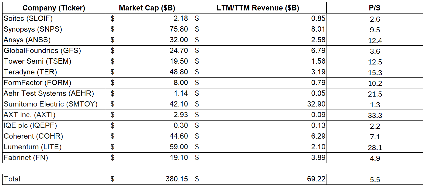
Don’t read too much into this, this is just to illustrate that the sector is still relatively small compared to the opportunity once CapEx flows down onto photonics - although obviously the entirety of the $0.5T won’t flow to optics, but even 0.5% of this total spending would be material for this sector.
There is no knowing exactly where the industry is heading. There’s lots of optimism and anticipation in the stocks today, with most of those names up hundreds of percent over the last few quarters, but there is a reason for such a performance and no saying where it stops. Some of these companies are still small caps, ignored by most of the large players because it is too early in the cycle to pour hundreds of millions on them, and analysts don’t even know half of them - even less their potential.
If you were to look at analysts’ expectations on Nvidia, they were wrong almost every quarter - still are today. Why? Because it was impossible to understand the sector and anticipate demand for their hardware and the spending frenzy which was unlocked over the last years. Some things cannot be modelled.
They aren’t stupid, they are simply playing a game which cannot be played as Nvidia - and AI, is an irregularity in the markets, a company and sector you only see a handful times in a lifetime, but it isn’t the only one and even if photonics names ran 500% over the last few quarters, nothing says they have reached their potential. It took Nvidia 1 year and a half to return 500% after being known as a key AI player and delivering its first GPUs to OpenAI in 2016. The stock is up 3,000% since.
I wouldn’t expect photonics to become Nvidia. But if photonics were indeed the next foundation for AI scaling, analysts won’t be able to anticipate growth, profitability and cash generation just like they couldn’t with Nvidia, because demand will be faster than they’d expect it.
Massive past returns do not mean future returns are unlikely. It means we missed the discovery, the riskiest part of investing where the potential is here but unconfirmed. It now is confirmed by Nvidia’s endorsement, while the potential is still unknown. If it were to be as transformative as expected by the market and Jensen himself, then the safest part of the gains are in front of us, with fundamental confirmations and stocks which should be lifted up by revenues, growth and cash generation.
The SiPho Supply Chain
SiPho: Silicon extraction → SOI wafers (Soitec) → EDA Simulation (Synopsys) → SiPho design (Broadcom, Marvell) → Foundry etching (GlobalFoundries, Tower Semi, TSM) → Testing and validation (Aehr Test Systems, Teradyne, FormFactor).
Silicon Extraction & SOI Wafers
Key player: Soitec.
Wafers are the foundation of all semiconductors, the platform on which elements can be etched or deposited. You can think about them as your plate during dinner, on which you will serve your dinner - except your food isn’t microscopic hopefully.

I have a detailed write up on Soitec, its business and its importance in the supply chain. They manufacture SOI wafers - a very specific wafer architecture optimized for photons, which are the industry standard for SiPhos, and not only do they manufacture them but they also own the patent for the industry standard technology to do so.
They are the first bottleneck of the «chain: every SiPho requires an SOI wafer which will either be produced by Soitec or by its partners who pay a fee to use their proprietary technology - except if buyers accept to pay more for another provider not using Soitec’s technology but that would be less scalable.
Investing wise.
As noted in my detailed review, Soitec is in the sweet spot to start an investment in my opinion - I own it, after a clear W50 breakout on massive volume after years of downtrend as its core business declined.
The market is ignoring its key position on the supply chain and focuses on the company as a whole, not on this SiPho position and revenue growth potential, which could eclipse the revenue decline in other verticals during the next quarters.
EDA Simulation
Key players: Synopsys.
The software providers. They do not design the chips, they build the complex digital physics simulators (Electronic Design Automation) that the architects will use to design the chips. Every single chip is first designed and tested within a software environment before sent to manufacturing, to theoretically prove the viability of the design.
Investing wise.
Synopsys has been part of the entire AI revolution as its software isn’t exclusively optic related which means its core business and revenue growth have already been rewarded in the past years. It remains a key player in the industry but I wouldn’t focus on it.
SiPho Design
Key players: Marvell, Broadcom.
The architects. Companies with the engineering capacities to design how light should interact within the SiPho to reach its maximum potential. They receive requirements from final users and work with them to design the most efficient SiPho for their needs, just like a house architect would design the best house based on your demands.
For the sake of clarity, while Marvell is only an architect - and specializes in optimized connectivity which is why it is such a key player in SiPho, Broadcom also has manufacturing capacities. Just to be thorough.
Investing wise.
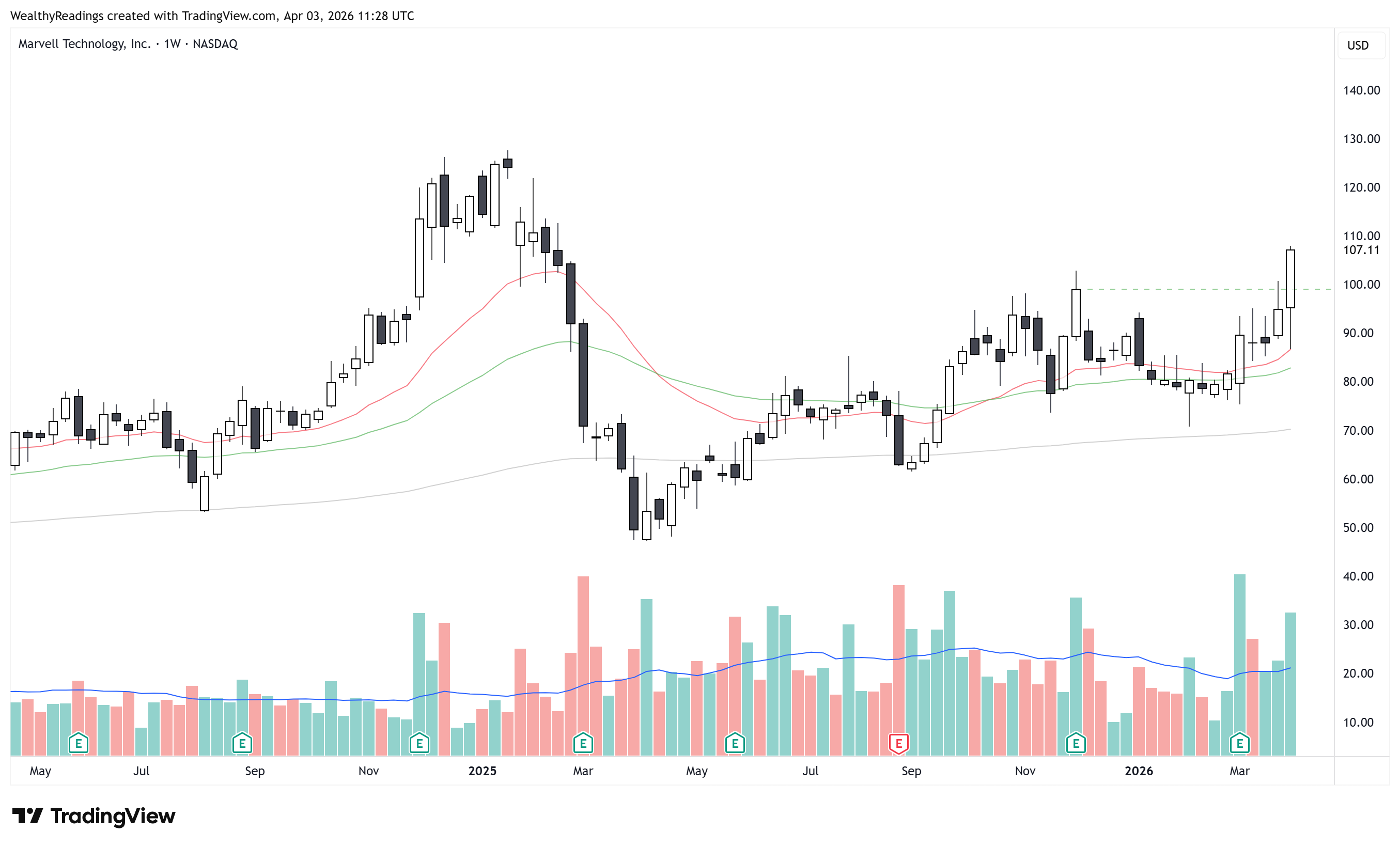
Just like Synopsys, both have been part of the entire AI revolution as their design aren’t exclusively optic-related, and both have been rewarded although Marvell was left behind as its core focus is networking - despite other verticals, which might give the company a push now as they will receive orders to fit optics within hardware.
The stock saw a healthy breakout on large volume post Nvidia’s investment and any retest ~$100 seems like a great entry.
This would be my focus if I wanted a stable giant with upside, ignoring the small-cap risks; Broadcom is retesting its W50 this week which is always a great entry during uptrends, but at a much higher valuation due to its partnership with Google for TPU designs. But a W50 is a W50, all great companies deserve to be bought at this level and any optics-focused partnerships - especially for Google’s TPUs, would push the stock even higher.
Foundry Etching
Key Players: GlobalFoundries, Tower Semi, TSM.
Just like Soitec, I have a detailed write-up on foundries.
Those foundries will etch the required components from the SiPho designs - waveguides, photodetectors, modulators, etc… on SOI wafers. These companies own fabs around the world and manufacture the finished product based on specifications.
Investing wise.
Tower Semi is up 290% since 2025, boosted in 2026 by Nvidia’s partnership, and is extended now. The opportunity is real but I wouldn’t touch such a chart, especially while they are being sued by GlobalFoundries for using patented technologies.
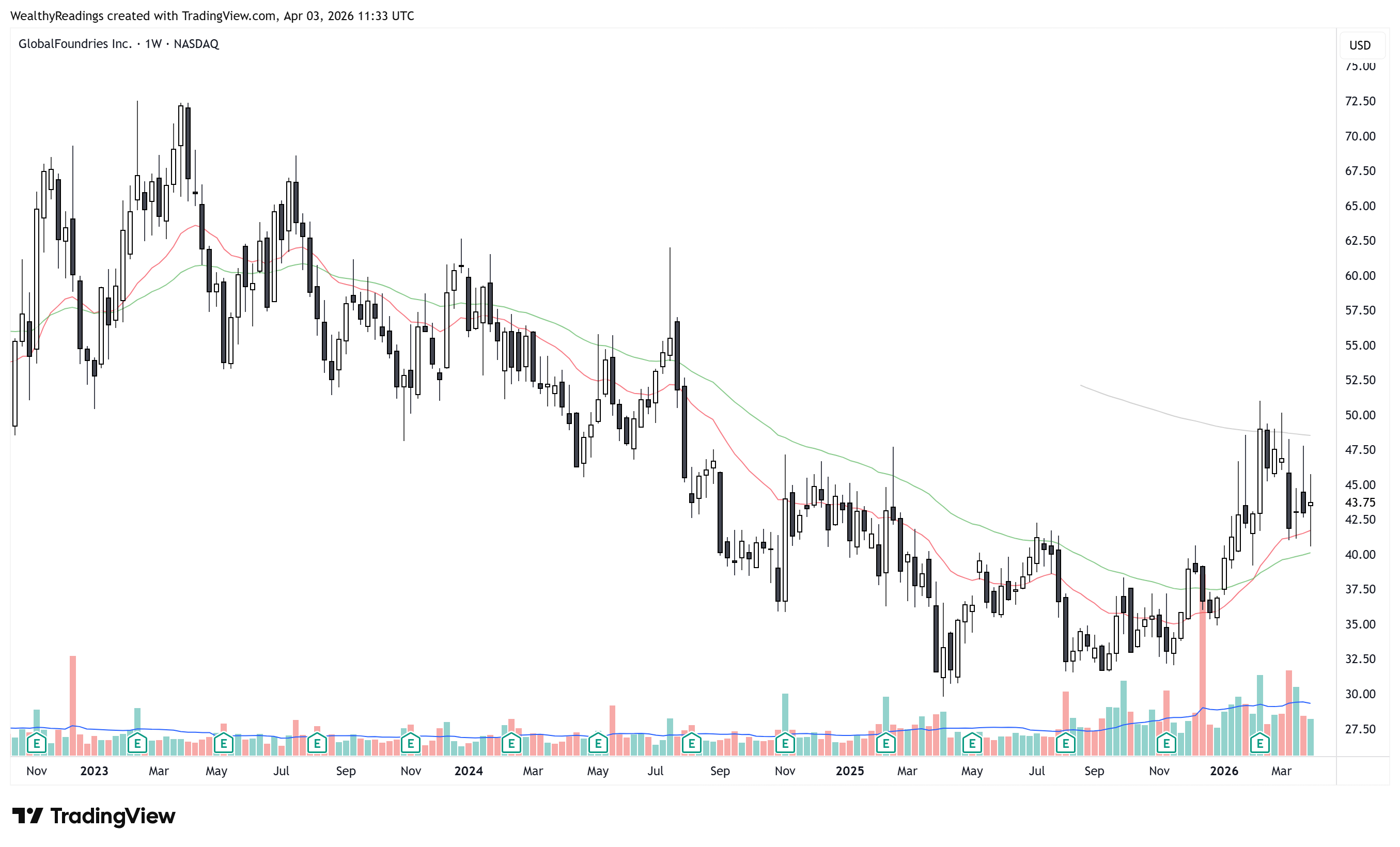
Both companies are key for optics and one is much cheaper than the other while having comparable potential. Just like Soitec, GlobalFoundries is dragged down by its core slowing business as it isn’t a SiPho pure-play, and is a much bigger company than Tower.
To me, GFS is the right play today with the perfect chart signaling accumulation at low valuation with a perfect retest of the W50 given this week ~$42, the price I highlighted in my review.
Tower would be a great name to own after a breather and TSM, which is obviously a great name, is also a major player for every semiconductor and a great opportunity but not a company I would focus on personally as I’d rather look at higher potential and volatility. As with Broadcom, a great focus to limit risks and volatility.
Testing and validation
Key players: Aehr Test Systems, Teradyne, FormFactor.
Once a semiconductor is finished, it must be tested as it won’t be shipped/paid for without confirmation of its performance. These companies sell the go-to systems or/and the components to test SiPhos components - and lasers as we’ll see later. They do not necessarily perform the tests themselves but usually sell the hardware to do so.
Investing wise.
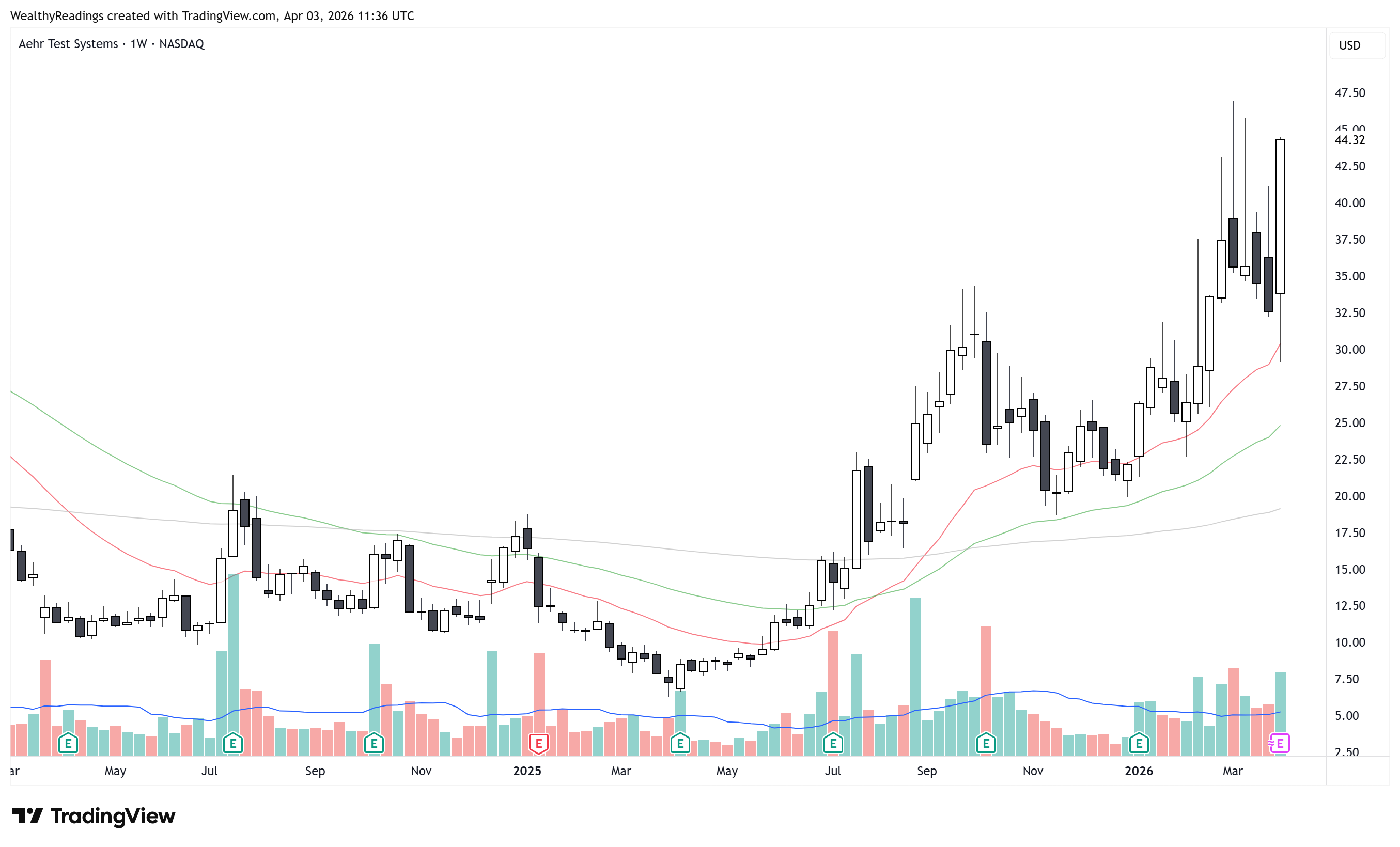
AEHR will be the best play fundamentally as the most used hardware to test optics and SiPhos (with wafer-level burn-in), and the market rewarded it. As with any uptrend, buying the W50 is key and AEHR gave many retests over the last months, waiting for another one is the logical next step to me.
Teradyne and FormFactor are both extremely extended at the moment, patience will be key on those to avoid taking the elevator down and seeing a position destroyed because of FOMO. But those three names would be great opportunities at the right price be exposed to the SiPho testing sector which should also see demand grow as production increases.
The Laser Supply Chain
Lasers: Indium/Phosphorus extraction → InP substrate production (Axti, Sumitono) → Epitaxy (IQE, Coherent, Lumentum) → Laser Chip Fabrication (Coherent, Lumentum) → Testing and validation (Aehr Test Systems).
I will not go over the raw material extraction as most of the production comes from China and the refinement of the material is then done during substrate manufacturing, so we’ll start there right away.
InP Substrate
Key players: Axti, Sumitomo
This is the name given to a wafer made from a different chemical (Indium Phosphide). Concretely, it remains a wafer, optimized for laser usage.
We will focus on Axti, which is comparable to Soitec. InP substrates are the industry standard for semiconductor lasers - yes we are talking about semiconductors which produce light (photons), Axti owns patent for specific process within the InP industry standard manufacturing technology called Vertical Gradient Freeze (VGF) which allow them to yield low-defect wafers and therefore cost competitive. And while this is their most important advantage, it isn’t the only one.
They also own the raw material extraction vertical through subsidiaries in China which gives them privileged access at a preferential price. Their operation in China aren’t just material extraction, they also manufacture InP substrate there which reduce costs massively and increase its competitiveness and their manufacturing scale.
Axti is the only InP substrate vertically integrated pure play and the very best in the entire market, meaning most of lasers demand for SiPho optical connectivity will pass through them at one point due to their prices.
Investing wise.
Without much surprise, it comes at a premium but this is where my speech about Nvidia and analysts’ expectation comes into play. The stock is up 2,222% since 2025 to a ~$3B market cap for ~$90M of revenues. It is extended, very much, but it has everything we are looking for: massive volume and rapid expansion on strong potential and fundamentals.
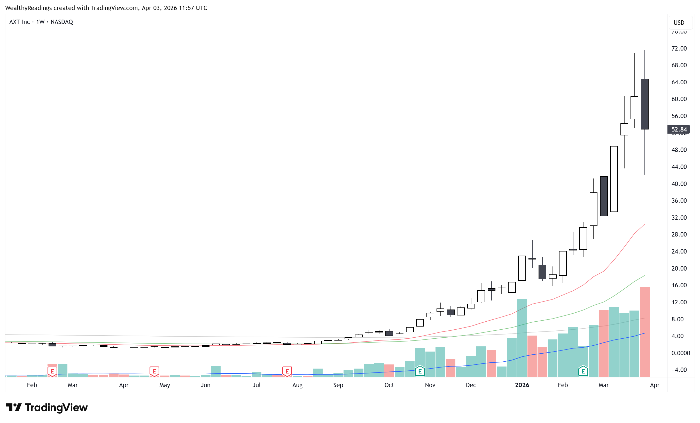
I would not buy here, but it is and will be a leader in photonics, one of the key players and most important company to scale optics within hardware, without any doubts, while having massive exposure to… China. Volatility will happen and as usual: the W50 is key in uptrends.
Massive past returns do not mean the run is over, it means we should be patient and wait for those retests which always happen.
Epitaxy
Key players: IQE, Visual Photonics, Applied Optoelectronics, Coherent, Lumentum.
We have a blank InP substrate, a perfect, flat crystal which cannot generate photons by itself. We need something else, a phenomenon called electroluminescence; epitaxy is the technological process to achieve it, by depositing microscopically thin layers of crystals on top of our InP base, called “Quantum Wells”. The finished product will be called an epi-wafer.
That’s where physics is amazing and our understanding of it is mind-blowing.
Here’s how those wells work. Electricity will be conducted within the hardware and electrical impulses will enter the quantum wells, which are designed to change the energy state of electrons and force the release of a photon. This is how a “simple” well generates light from an electrical signal.
IQE and Visual Photonics are the epitaxy leaders, I added Applied Optoelectronics, Lumentum and Coherent because all three also do epitaxy - but not only as we’ll see below. When it comes to pure epitaxy needs, a fab to transform InP substrates into epi-wafers, IQE is the western leader.
Investing wise.
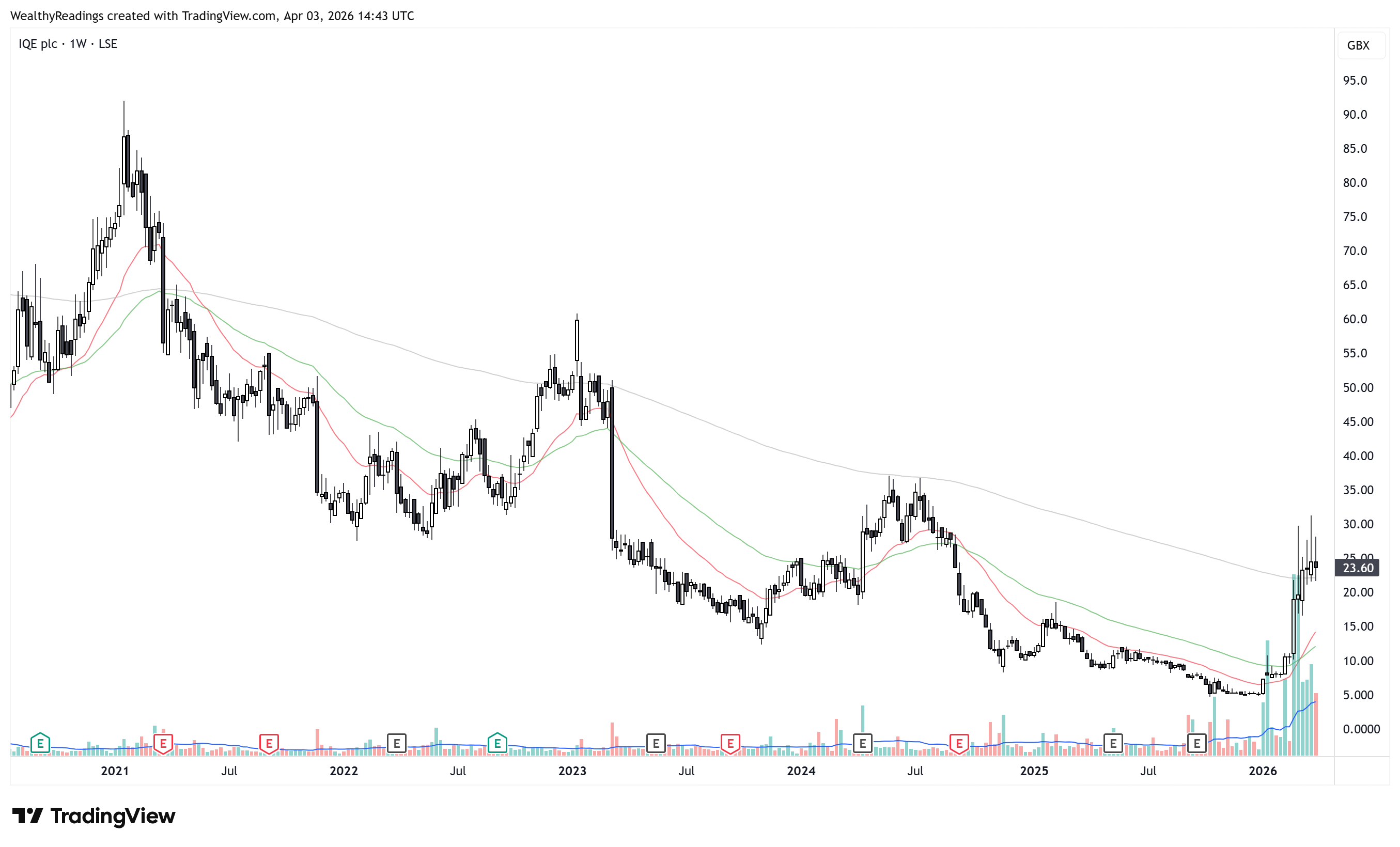
It won’t surprise you if I tell you that IQE is up 382% year-to-date I guess. And yet, compared to the rest of the sector this isn’t much as the stock is only up 122% since 2025, while being the go-to company for epitaxy. The stock has been on a downtrend since 2017 as the need for epi-wafers was very niche and never met expectations, until this year, with demand for lasers growing.
If the thesis of this write-up is right - that photonics are the future, then epitaxy is a mandatory step to scale it. The question is: will it pass through dedicated fabs or vertically integrated ones? In the first case, IQE has a long way to go, although the company has other structural issues that any investor should look at before investing - this write up is focused on the photonics supply chain not individual financial profiles.
Laser Chip Fabrication
Key players: Coherent, Lumentum, Applied Optoelectronics, Sivers Semi.
The last step of the chain, which consists of many different actions including etching waveguides, cleaving the wafer into individual laser chips, adding conductive metals, etc… This is the equivalent of the SiPho’s foundry stage, once the wafer (epi wafer in this case), is ready and the final touches are missing to manufacture the finished product meeting clients’ specifications.
We can find names we already know; those companies are vertically integrated, they do their own epitaxy from the InP substrate, they work on the design and the final touches on the wafer - they do not need to pass through IQE or other fabs, they do it themselves.
Once treated by one of these companies, the InP substrate leaves the factories as a finished and functional semiconductor laser which can then be packaged with SiPhos to offer a complete optical connectivity within hardware.
Investing wise.
As you can imagine, those are loved by the market as vertically integrated on one of the most important sectors to develop and scale photonics. They are extremely extended today and could remain like this for long, but they will be key in the development of photonics and any retest on the W50 would be a buying opportunity as long as it happens on healthy fundamentals - not the rejection of their technology.
Testing and validation
Key players: Aehr Test Systems, Teradyne, FormFactor.
We already went through them as they propose complete testing systems - which include both the lasers and the optic channels.
CPO Packaging
Key players: Fabrinet, Coherent, Applied Optoelectronics, Lumentum.
We’ve seen all the key companies required to manufacture both SiPhos and lasers, the only step missing is to combine both technologies into a packaged solution capable of delivering a customized optical connectivity within hardware.
The industry will rely on pluggable optical transceivers for the next quarters until the final product, Co-Packaged Optics (CPO), is ready to scale but both will use the same components so the supply chain is identical.
Packaging is probably the most important step of them all as electrons don't care if a copper wire is slightly crooked, but photons will miss the target if a laser is misaligned with a silicon waveguide by even a fraction of a micrometer - and the device will be useless.
We find our three leaders once again - vertically integrated laser semiconductor manufacturers as advertised. The only step they do not perform is the creation of the InP substrate, which they will always need to purchase. But we also find another company: Fabrinet.
The known giant and the only technology-agnostic one as the company receives the required products/specifications and assembles them as required by their final client. This technology-agnostic giant has the advantage of flexibility.
Investing wise.
The stock has been rewarded for its packaging services globally, up 142% since 2025 as the company is much larger and exposed to more optical verticals than just these new technologies. Another large and stable company to invest in for those who want to avoid small caps.
Conclusion
The photonics sector is just starting. Many of these names, which are still ignored by most market participants, will accelerate once real revenues and continued orders flow really kicks in. We’ll need to buy them at a correct price but the thesis and the signals are strong, execution is the only missing link to have successful investments.
This write-up was designed to give a complete overview of the entire AI optical supply chain, from raw physics to hardware, from blank substrates to pluggable transceivers and CPOs. The complete supply chain to replace our congested copper highways with light/photons.
Keep in mind those companies are part of the same sector but all have their particularities and financial profiles, their own risks. Depending on whether you want to invest in them long-term or simply trade them by buying key support levels and moving averages you will need to do your own research and follow your own process. I am here to share the ideas and the logic behind the narratives only.
Personally, I intend to wait for key supports on daily/weekly charts. I intend to take small positions with a trading mindset - clear entry and exit points, while waiting for deeper breathers. Hopefully, we’ll soon see pullbacks on their W50 where, if the fundamentals stay as strong as today, I’d build heavy positions in those names and ride the entire photonics wave - while I already have large positions in GlobalFoundries and Soitec.
I hope this write-up gave you a bit more clarity on the supply chain, the key actors and the fundamentals of this massive new AI vertical, and that you will be able to leverage this information into your own systems.
There’s always a bull run somewhere.
Disclaimer: I am not a licensed financial advisor, analyst, or broker. This content reflects my personal opinions and investment decisions for informational and educational purposes only. I hold positions in securities discussed and may buy or sell without notice. Nothing here constitutes a recommendation to buy, sell, or hold any security. Past performance does not guarantee future results.
Always conduct your own research and consult a qualified professional before making investment decisions. I accept no responsibility for any financial losses.
Saving for later!
I bought in Soitec, Sivers, and AAOI. The sector is so compelling. the upside potential is massive, and the market hasn’t fully caught on yet.. investors seem to be lagging behind even though memory, Neoclouds and GPU set the stage