
The Photonics Monopoly
The socle of the next AI innovation cycle

Introduction & Semiconductor Basics
We’ll need to go back to some basics to have a proper understanding of our subject: semiconductors. We’ve talked about all this already on my ASML/TSM review so go for it, it’ll be a great introduction, even though we’ll go over the basics again today.
What are they? Simply put, they are etched circuits on wafers. The complexity comes when we start talking about the circuits – which are meant to conduct electricity between components, and the wafers – which are made of different elements to optimize conductivity or not.
The final goal of any semiconductor is to control current between elements being cautious on signal clarity, speed and heat, which results in different circuit pattern, elements, components, materials, etc… Hence their complexity and constant improvements, as they are also very, very small - we’re talking ~1,000 time thinner than a hair.
This explains why we have many different components and how critical they are. The objective of a semiconductor within a smartphone isn’t the same as within a 5G antenna which again isn’t the same within a GPU. They’re all different in size, components, materials, etc…
Which brings us to our subject today, a new kind of semiconductor we talked about a few days ago in my GlobalFoundries and my Silicom Ltd thesis: photonics (optics semiconductors called SiPho for Silicon Photonics) and their packaged version CPOs (Co-Packaged Optics) which are the aggregation of SiPho within a board to make it usable. Those are the new innovation supposed to push AI datacenter capacities further and solve the actual networking bottleneck.
And as for any semiconductors, it all starts with the wafer.
SOI (Silicon on Insulator)
The wafer is the raw platform made from specific materials on which circuits will be etched; SOI is one kind of wafer, optimized for optical connectivity, hence bandwidth/latency. A “normal” semiconductor is a simple layer of silicon. The problem is that silicon is transparent to some wavelength, not usable to transport light by itself as it would pass through it left, right, top and bottom, losing photons to the void hence signals, data. Not very optimized…
No, for light to transit, we need it contained within a defined and reflective space so no photons are ever lost as they bounce until they reach their destination.

This is how it works in optic fiber for example, which can look weird as it is nothing but a twisted cable plugged between two pieces of hardware. In reality, the light bounces on the refractive side walls of the cable until finding the receiver at the other end, without losing a single photon in the process – nothing affecting data transmission at least, and with no heat.
If the cable was made of silicon only, the light would pass through…
When it comes to optics semiconductors, we use SOI wafers, a three-layer cake optimized to trap light where we want it: within the silicon only. SOI are manufactured with a technology called “Smart Cut” which is a patented method from the company we’re talking about today.
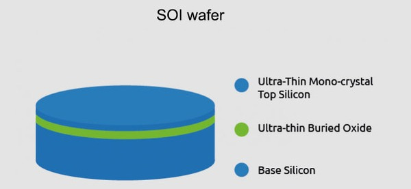
Here’s how they work.
Layer 1 – Single-crystal Silicon. Classic semiconductors, except instead of etching conductive patterns for electrical impulse, we will etch “waveguides” for lights to refract and follow a direction, just like in an optic cable.
Layer 2 – Buried Oxide (BOX). An oxide layer more reflective than silicon which prevents light from escaping below the silicon layer.
Layer 3 – More silicon. A much thicker meant as a handler. A mechanical layer to fix the wafer and give it stability; we are talking about a semiconductor optimized to let light pass through, precision is necessary.
When connected to a light source, photons will transit through the semiconductor, trapped between “waveguides” etched on the first silicon layer and the reflective BOX around, between point A and B with minimal loss and heat.
SiPho are optimized for bandwidth and latency and when packed within a CPO, they give the possibility for data to transit through photons within a GPU, a rack, or any other hardware, pushing AI compute to a new scale.
Now again, what we call SOI is only the wafer which will be sold to a foundry to be etched according to specifications into a SiPho, then shipped or directly assembled within a CPO and installed within a GPU, rack or any kind of hardware which requires optical networking.
The wafer is step 1 of a semiconductor’s life (excluding material extraction and refinement), GlobalFoundries and Tower Semiconductor for example are buyers of wafer to etch them, build CPOs and resell those finished products. You know I am bullish on SiPho, CPOs and on both foundries so very logically, I am bullish on demand for wafer.
SOI Usage
To do a bit of history SOI isn’t new, has been used for years and is very critical in sectors which are already focused on optical connectivity.
RF and mixed-signal devices (4G/5G, smartphones, satellite communications…)
Low-power and high-performance CMOS (AI datacenters, wearables…)
MEMS devices, including sensors and actuators (cars, medtech…)
Power management ICs (EVs, IoT…)
The AI datacenter need is new as no one foresaw a decade ago that our network would be a limitation for global compute withing hardware, creating a bottleneck. The tech industry realized this maybe a few quarters ago and needed time to engineer the solution, which is coming to life nowadays in the form of massive and growing demand for SOI wafer and SiPho.
Soitec Dominance
Now that all introductions are done and we understand SOI and their applications, we can talk about Soitec, which is the leader in SOI wafer. I’ll be very straightforward, not only are they the leader, they own the technology on how to manufacture SOI wafers which gives them a quasi-monopoly on who can and cannot do so.
Two words: Smart Cut, the technology used to create the BOX layer within a silicon.
Yes, Sebastian, on the overall SOI market, of course, there is. We always say that there is competition, starting with our only licensee today, with SEH. But we don’t see big changes in the segment shares we are observing, and particularly for us, regarding the 200 and the 300 millimeters. Of course, players are claiming to have SOI solution, and some SOI solutions are not using our technology like Smart Cut. You can have also other ways to do SOI, a silicon insulator, namely BSOI, that is quite well adapted for power application in the cars. But even the domains, competition, and our positioning, it’s quite strong.
Then today, we don’t see segment shares, significant evolution, and the competition is far away from what we are doing.
Pierre Barnabé, Soitec Q4-25 Earning Call
As you could read, it isn’t the only method to manufacture SOI wafers, another main one being SIMOX (Separation by IMplanted OXygen). The objective and results are the same but as the method is more complex and more expensive due to the hardware used, and as no one wants to pay equal quality more… well, the cheapest and most scalable wins.

And that lays my investment thesis on Soitec; they are the company owning the patent to manufacture the cheapest SOI wafers at scale, which usage is supposed to blow up as SiPho and CPOs demand is also blowing up… What’s left to say?
This doesn’t mean they are the only producers of SOI wafers, others also do but have to pay a fee for using their technology so Soitec effectively makes money on 100% of SOI wafers manufactured with Smart Cut, plus their own production which is ramping up, with accelerating orders, demand and contacts from the tech industry.
Edge and Cloud AI revenue amounted to EUR 54 million, showing 27% organic growth YoY and improving from Q2-26. Activity continues to be supported by AI-related demand across edge and cloud environments, with contributions from both Photonics-SOI and FD-SOI. Specifically, Photonics-SOI remains very dynamic.
And today, we have more than five customers today engaged in our silicon photonic solutions, and more and more are coming.... And each of these customer asking for more and more volumes. I’m confident that this dynamic should last, because the need for AI are very important. And of course, we are part of this components of this industry, because the silicon photonics is today the only solution, viable solutions, that is allowing for next generation AI data centers, transfer control, to transform, electron into photons for high bandwidth. Particularly if you move up to 1.6 giga. Not only for the data centers, but tomorrow to interconnect the GPU, and particularly with the co-packaged optic solutions.
And on top of it, we are enhancing our photonics layers with the lithium niobate, let’s say, add-on, that is helping the industry to move beyond the 1.6 tera. That means that we have today a plan, a clear plan, and the industry have a clear plan to fuel the silicon photonics growth, for the coming 4-5 years, without any doubt. And our market shares, positionings, relationships with our customers, is making us confident.
Pierre Barnabé, Soitec Q4-25 Earning Call
Besides these confirmations from Soitec, we have confirmations on SiPho and CPOs demand with companies like GlobalFoundries and Tower Semiconductors talking about a ~50% CAGR in SiPho and expansions for their SiPho fabs – a $900M expansion planned this year to 5x their production for Tower while GlobalFoundries is planning to increase production after their acquisition of Advanced Micro Foundry to a $1B+ run rate by end of year 2027 - hence roughly 4x as well.
Very basic math, if Tower and GlobalFoundies both intend to 4x/5x their production in the next two years or so, it also means they will need to 4x/5x their SOI wafer purchases and as we’re looking at industrial scale, most should be produced with Smart Cut which means directly sold by Soitec or by companies paying fees to use Soitec’s technology.
I think you start to see the potential already.
The Opportunity
I won’t be able to put a price or a target/valuation on Soitec because we are talking about the company potentially responsible for the next AI datacenter innovation, the first wheel of a car which should be very fast. It’s impossible to anticipate demand, revenue growth, margins nor the potential premium which could come from their position, so I won’t it. It’s also hard to anticipate how the stock would react if CPOs weren’t the solution and demand for SOI wafers were to fall.
What I can say though is that today, Soitec is in the same state than GlobalFoundries: completely ignored by the market because of its slowing core business, looking like a weak company with declining growth and margins, unprofitable and certainly not worth any premium.
Why? Because they are the leader in SOI wafers and those are used in other sectors, AI datacenters are only the new shinny source of demand, while the other sector… Well, they’ve been extremely weak and plagued by an inventory building during/post Covid, as the period boosted demand for hardware which slowed down massively the years after.
In mobile communication, customer engagement remains active around advanced RF solution and next-generation platforms, despite constrained volumes with RF-SOI demand still impacted by customer inventory correction, mobile communication generated revenue at EUR 90 million in the third quarter, down 36% year-over-year organically.
In automotive and industrial, while the environment remains challenging, our technologies are well-positioned to support future applications once demand recovers. Automotive and industrial revenue reached EUR 16 million, improving sequentially versus the second quarter, but remaining down 32% organically year-on-year. Market conditions are still weak.
5G activity was slightly down year-over-year, while showing an improvement from Q2.
On a year-on-year basis, revenue remains down, reflecting a 22% decline at constant scope and foreign exchange, and a negative currency impact of 7%. Sequentially, revenue increased 18% organically compared with the second quarter, coming in above our guidance.
Pierre Barnabé, Soitec Q4-25 Earning Call
If that remind you another story – and opportunity, this is the exact same situation for Nordic Semiconductor.
Soitec is going through a rough time for the biggest volume of its business which is mostly for RF technologies, cars and smartphones – with the last two being in a clear slowdown/stabilization since Covid hence inventory issues and slow demand recovery, which in turn triggered slow growth over the last years.

Management was a bit more confident this last quarter might be close to demand bottom, but this wouldn’t mean return of growth on a their core vertical this year and would still hurt the profile of the company.
As for inventory reduction, which is another priority, we’re aligning production with actual demand. Of course, the downside of this is that it brings a temporary hit on margins and profitability.
Pierre Barnabé, Soitec Q4-25 Earning Call
In the middle of this situation, we have an SOI organic growth for photonics up 18% sequentially and 27% YoY combined to very positive management comments on what is yet to come and their capacity to deliver in volume with strong supply chain for materials – which will be my next area of research as if demand for SOI wafers grows, demand for materials also will and might create other opportunities, combined with lasers as transporting photons happens only if photons are generated (to give you a heads up on the potential next narratives).
We have no specific limitation, but to be sure, we organize properly our factories, because of course, we are sharing the same factories for the 200 and particularly the 300 millimeters. Then it’s a matter of anticipation. But we have access to the right level of bulks. As you know, we diversified also our sources of silicon bulk in terms of the quality, and particularly the one able to correspond to Photonics’ requirements and demands. We have today more and more customers asking for Photonics and more and more in volumes, 200 and 300 millimeters. But today, there is no specific limits to take the ride and to accompany a market that is growing by around 25%-30% per year.
Pierre Barnabé, Soitec Q4-25 Earning Call
This is the global thesis on Soitec today. A company trading at low valuation because of low growth and declining margins due to a slowing core business, with the potential to be revigorated by a massive and accelerating demand for their wafers for photonics, on which they have a quasi-monopoly as they own the patent to produce them.
This looks like a pretty strong potential here.
Investment Plan
You should be used by it now, the chart looks like every charts I look for. A clean base – although this one was pretty rapid, built in ~4 months, with a lower low on massive volume followed by stable price action on growing volume, which indicates more buyers at actual price, meaning the majority of the market finds value at this price – otherwise price would drift lower. And as usual, the final confirmation comes from a breakout and reclaim of the W50 on volume spike, meaning most of the market accepts, in sync, to pay more for this stock.
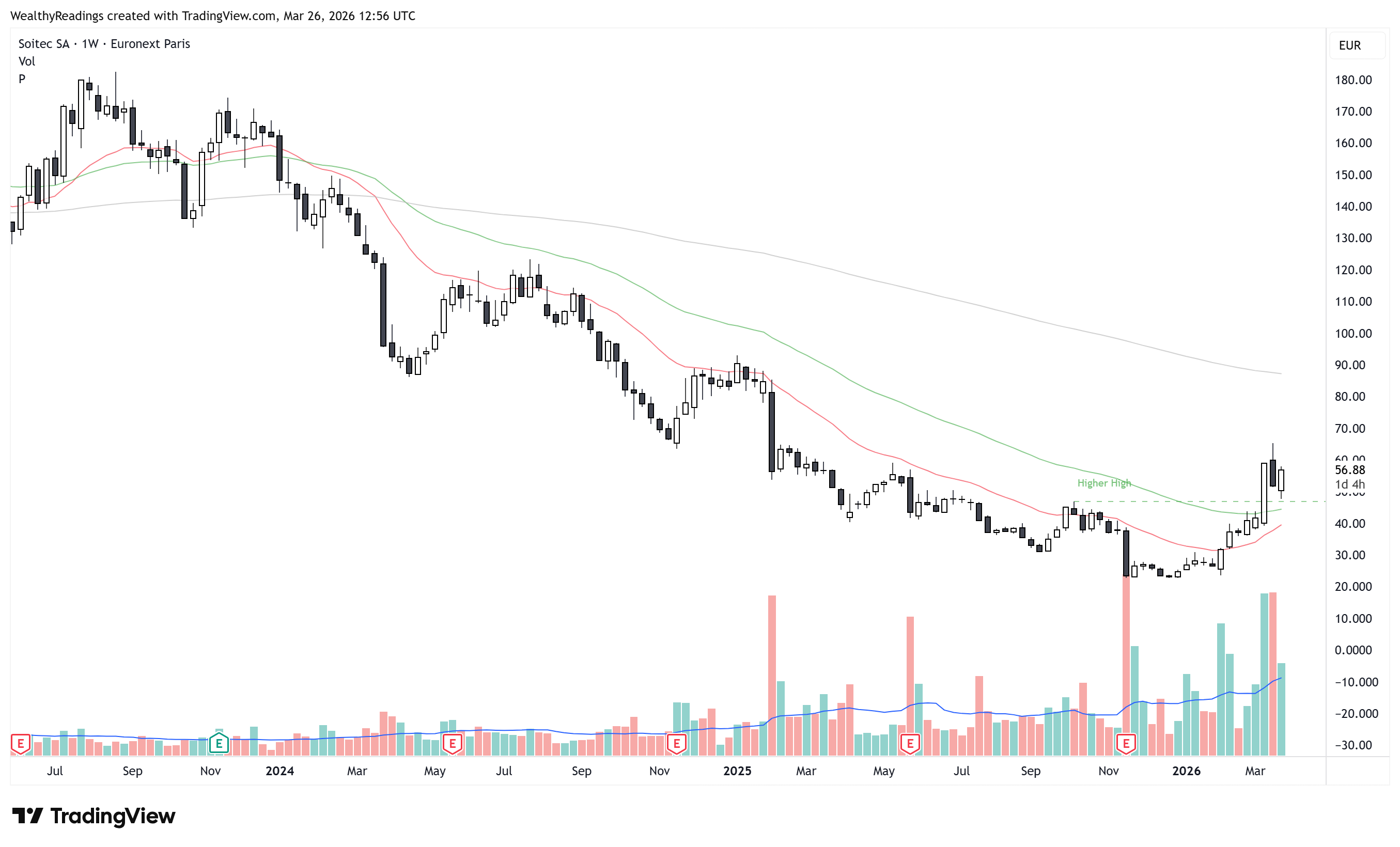
There are always reasons for liquidity to go towards a name: value and potential. It doesn’t mean every stock with this pattern will succeed, but every success starts with this pattern because a large base of investors accept to pay higher prices for the stock and bet on its success. And that’s what we want to see - and buy.
We now know why those investors bet on Soitec, our next step is to know if we want to be involved with it and at what price. I want to and bought on Tuesday as the French market had a bad day and Soitec followed – yes Soitec is a baguette company. That retest went close to the W50 and I built a pretty large position, as a concentrated investor buying a great price target.
I shared this on my Silicom Ltd write up because of the volatility of this name and was right to as it went up double digits since. I couldn’t write fast enough in time…
Once again, it is very hard to value the company and set targets - to buy or sell, as we have no idea of the wafer volume coming their way nor their capacity to execute. Soitec has never received a premium comparable to their situation today, so we can’t really model anything. This is a narrative trade with a massive potential, which could materialize - or not.
My opinion is that a EUR 1.81B company trading ~2x sales with the potential to become a critical infrastructure company for the future of AI datacenter has upside, both in term of growth and premium valuation - hence pretty explosive upside. And is actually trading at a pretty sweet spot even considering its core business – which is supposed to stabilize, compared to historical multiples.

The real risk lies in the success on SiPho and the continuous dominance of Soitec in the SOI wafer vertical. I wouldn’t touch this stock otherwise. If CPOs weren’t working or weren’t the answer to the actual networking bottleneck, or if a competitor were to find a better technology than Smart Cut, this investment could hurt, badly. There are no answers on the CPO efficiency yet – although the entire industry points to it but things could change, and when it comes to dominance, Soitec is ready to defend its position and even consolidate it with more patents.
We are filing more and more patents every year, more and more. This year we're gonna even beat what we did last year. That was quite exceptional. Then we continue to run ahead.
Pierre Barnabé, Soitec Q4-25 Earning Call
But the risks exist.
As I said I am already in and will gladly buy more if we see another retest ~W50, I only bought commons; I do not do options on such names. Low valuation and expected volatility are the perfect recipe to blow up option trades. No reasons to add risk on an already risky trade. Only shares with quarters long timeframe - hopefully years.
If SiPho and CPOs are indeed the future of AI datacenters as many – Jenssen included, believe, then we’re probably in for years of growing demand, and if AI hardware were to indeed need to include CPOs in each of them… There is a case to say that SiPho and CPOs will be the next biggest vertical of AI hardware, and we know hyperscalers aren’t done spending.
If that were really the case, then the need for SOI wafers would only be starting and demand for it would only accelerate.
Then the co-packaged optics is, is really a new architecture, for which we see, some, pull forward, because, it was expecting to come in 2028, then 2027s, and today we, we have heard that, some, first, let’s say, design gonna be, gonna be commercially available by end of, of this year. Then there is a clear accelerations.
Pierre Barnabé, Soitec Q4-25 Earning Call
If so, then the next innovation cycle relies on SOI wafers.
And then, mostly on Soitec.
Disclaimer: I am not a licensed financial advisor, analyst, or broker. This content reflects my personal opinions and investment decisions for informational and educational purposes only. I hold positions in securities discussed and may buy or sell without notice. Nothing here constitutes a recommendation to buy, sell, or hold any security. Past performance does not guarantee future results.
Always conduct your own research and consult a qualified professional before making investment decisions. I accept no responsibility for any financial losses.
appreciate all the free alpha. Ignore the dummies on X.
A first class breakdown - no noise!!
Keep up the great work - appreciated 👍