
ASML & TSM | Investment Thesis
The microchips monopoles.

My objective over the next weeks, months & quarters will be to increase my position on AI hardware-related companies. Which means more content will come your way about those companies.
We’ll start by ASML today, the perfect subject to cover the basics as ASML is the start of everything. By extension, this write up will also cover Taiwan Semicondutor as both are closely related - and any other microchips fab at least for their fundamentals.
Microchips, or semiconductors, are one of the most unknown & yet present hardware in our daily life.
In 2021, semiconductor unit sales reached a record 1.15 trillion shipments. That’s about 145 chips for every person on earth.
They are at the heart of the AI revolution as what made AI models possible were the improvements on semiconductors, more precisely the improvement of compute per unit which unleashed a torrent of innovations in our world.

And we are far from over as AI is rapidly being updated, used in new domain, for new use cases, all around the world… The pace of innovation is accelerating, and it’s all thanks to lithography, microships. Semiconductors. GPUs. ASICs. And more.
Semiconductors. Chips. GPUs. Nani?
Let’s try to make sense of each.
We’ve heard non stop about semiconductors lately, but what are they really? The simple answer is that they are materials with electrical conductivity. The most known, and the most used, is silicon, a semiconductor born from sand - the silica contained within sand to be more precise, which is extracted & purified to give silicon.
It is the most versatile semiconductor we have and can be mixed with other materials - phosphorus or boron, to modify its conductivity. Sand being an abundant resource on earth makes silicon an even better candidate to mass usage.
Silicon being the base material used to create microchips is the reaon why we usually call those semiconductors.
This mix of silicon & co is thinned into wafers and modified through different process in order to imprint patterns - circuits and transistors, which will act as conductors and switches to let electrical flow transit through the chip as designed.
Microchips are made by building up layers of interconnected patterns on a silicon wafer. The microchip manufacturing process involves hundreds of steps and can take up to four months from design to mass production. In the cleanrooms of the chipmakers’ fabs (fabrication facilities), air quality and temperature are kept tightly controlled as robots transport their precious wafers from machine to machine.
This is what a finished microchip or semiconductor looks like, a multitude of “tiny skyscrapers” as ASML would call them.
Microchips are made by building up complex patterns of transistors, layer by layer, on a silicon wafer. Modern chips can have up to 100 layers, which all need to align on top of each other with nanometer precision

The size of a chip varies depending on the need but is usually around a fingernail size, which should give you an idea of the size of the circuits & transistors imprinted on it, as there are billions of each on each chip.
Chip features are measured in nanometers. A nanometer is one billionth of a meter, or a millionth of a millimeter. For comparison, a human red blood cell is 7,000 nanometers in diameter, and the flu virus is around 100 nanometers. The most advanced microchips contain features that are just a few dozen nanometers in size.
And this should give you an idea of how insane and advanced technology is, as we have machines capable of engraving and creating circuits smaller than a virus.
Size matters as it dictates power capacity. Last decades’ objective was to manufacture smaller - or of equivalent size, chips with more components etched on each, hence a higher compute/size ratio. This explains the miniaturization of smartphones, laptops, datacenters, etc… The latter are still massive but the ratio computing power to size has never been better than today – and still improving.
Now that we know what semiconductors & chips are and are made of, we can move forward, talking about the different kinds of chips.
Logic.
Those are the brains of electronic devices. They process information to complete a task. This category will include CPUs, GPUs and nowadays NPUs (neural processing units, designed for deep and machine learning applications). We have talked about those on Nvidia’s investment thesis already.

To answer the original question, yes, GPUs are nothing but a type of chips.
Memory.
Those store information with two different methods: volatile and non-volatile. The first ones save data only while the device’s power is turned on - DRAM for example. The second save data even after the device is turned off - storage.
The first one will help electronic devices work faster as it remembers the last moments accurately while the second will remember your data for ever - your pictures or documents are probably stored in those memory chips.
ASICs.
Those are single-purpose chips used to perform repetitive tasks such as resolving mathematics operations, like to mine Bitcoin for example.

That concludes our introduction. Chips are everywhere nowadays, but before using them, we need to manufacture them.
Fabs, Fabless & TSM.
This is where we’ll talk about Taiwan Semiconductor, the best and most advanced chip manufacturer, but not the only one as we could also talk about Intel, Samsung, Texas Instruments, etc...
Those companies own fabs - chip manufacturing hubs, & manufacture chips for other companies, which are called fabless – Nvidia for example. Fabless companies engineer their chips in blueprints and send those requirements to fabs in order to manufacture them. Once again, the most advanced fabs are TSM’s, for a few different reasons, the main one being their reliability.
TSM only manufactures for others. They do not build blueprints for internal use like Samsung or Intel who use their own chips for in-house hardware. This allows TSM to accept any kind of demand without constraints. They focus on what works best and their clients’ needs, which allows them to achieve above industry yield – volume of functional chips after manufacturing, which is an crucial metric for their clients.
This also allowed them to move fast on R&D and rapidly develop and mass produce their 3nm chips which have been scaling rapidly the last quarters, with their 2nm coming soon enough.
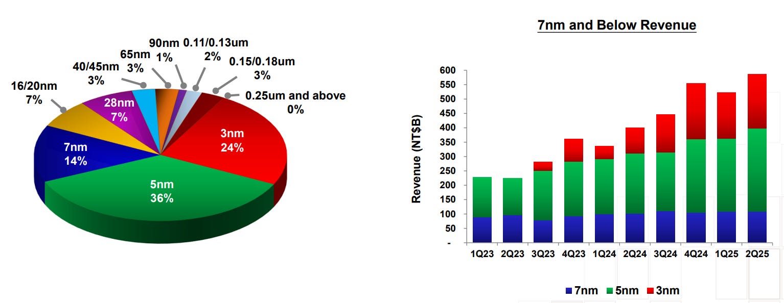
Once again, the more components on a same or smaller sized chip, the more power per unit of volume, hence the more demand as it’ll allow a comparable or superior amount of power for a smaller unit of volume.
Taiwan Semiconductor has the best infrastructures, the highest production yield, the best versatility to answer customers’ demands, the most advanced R&D & the most talented workers.
We know about silicon, semiconductors, chips, fab & fabless companies and why TSM is the best manufacturer. What we do not know is what ASML does?
Lithography, EUV & DUV.
The simple answer is that they manufacture the hardware which manufactures chips. As you can imagine, a nanometer wide circuit is not printed by an artist, it is printed by one of the most advanced machine there is, using advanced technologies.
Lithography.
I am not sure how interesting my own words would be, so I’d rather share ASML’s detailed explanations.
Inside the lithography machine, light is projected onto the wafer through the reticle containing the blueprint of the pattern to be printed. The system’s optics shrink and focus the pattern onto the resist. Where light hits the resist, it causes chemical changes, recreating the pattern from the reticle in the resist.
I will let you dive deeper on the process by yourself. This overview should be enough for the scope of this write-up.
We are talking about a level of engineering which cannot be understood by the likes of us and is dependent on so many verticals - optics, manufacturing, high-end R&D, commodities enrichment, software development… Not something which can be reproduced easily.
There are two kinds of lithography technology.
Deep Ultraviolet (DUV).
The DUV is the “classic” technology, known by any chip maker and built with specific lasers resulting in specific spectrum & wavelength. The latest developments in DUV hardware, called ArF, is built on lasers that produce light with a wavelength of 193nm.
Extreme Ultraviolet (EUV).
EUV is an ASML patented technology with a wavelength of 13.5nm.
EUV light occurs naturally in outer space. But to make EUV lithography possible, we needed to engineer a way to create such light within a system. So, we developed a radically new approach to generating light for lithography. In our laser-produced plasma (LPP) source, molten tin droplets of around 25 microns in diameter are ejected from a generator at 70 meters per second. As they fall, the droplets are hit first by a low-intensity laser pulse that flattens them into a pancake shape. Then a more powerful laser pulse vaporizes the flattened droplet to create a plasma that emits EUV light. To produce enough light to manufacture microchips, this process is repeated 50,000 times every second.
This technology is the only one capable of printing the most intricate patterns on the most advanced chips nowadays, hence the only hardware usable to push forward compute optimization - at least from a hardware perspective, highlighting how advanced ASML’s hardware is.
Both technologies work together with DUV being used for the “easy” patterns & EUV used for the “hardest” ones, resulting in an optimized workflow to manufacture the most advanced chips on earth.
This is why ASML is such a valuable company. There are no competition for its EUV system today, and while there are alternatives for DUV systems, chip manufacturers would rather rely on the same lithography provider for all its hardware as they are engineered to work together, and relying on different providers for such critical machines would create more issues which aren’t worth the costs saved.
Software.
This is about the hardware, but like with Nvidia’s CUDA, the best hardware can only go so far by itself, and software makes the difference between great & excellent.
ASML has some of the most advanced & precise software in the world allowing their hardware to correct the tiniest deviation or parameter variation.
Our scanner metrology software helps measure and compensate for sub-nanometer inaccuracies that inevitably creep in during production due to material imperfections, temperature fluctuations or atmospheric pressure changes. It calculates how our hardware should behave to correct for this, coordinating the many components to maximize system performance.
Data collection, machine learning and AI to optimize or filter this data and only collect the valuable portion of it in order to train & optimize their in-house models and at the end of the day, perfect their hardware and chips manufacturing.
Business Model.
As you understood, both companies are hardware focused.
The biggest bulk of ASML’s revenues come from shipping their DUV and EUV systems, which is why the market looks at the company’s order book closely - which has been pretty flat lately, as it translates demand and future revenues.
As their hardware gets better, they also get more expensive with an average of a few dizaines of millions for each, which once again explains why chips manufacturers rely on ASML for both DUV & EUV.

Hardware sales is 76% of ASML’s total revenues, the rest coming from different kinds of services with a 24/7 support, a 24h parts delivery, a training program, guarantees, more advanced systems, etc…
TSMC also has a pretty straightforward business model as they receive orders & wafer blueprints, manufacture them in volume and ship them to customers, with a steep increase of volume since June 2023.
The more interesting data for TSM is the sector demand for its wafers.

Without any surprises, we can see a stable demand from smartphones - in terms of volume but for more advanced hence more expensive chips, and a rapid increase of demand for HPC which is related to AI use cases.
As you understood, part of TSMC’s expenses go directly to ASML as they use their lithography hardware to produce those chips.
You can also notice both companies have a cyclicality in term of demand, mostly due to technology improvement timings. As more advanced chips are engineered, more power can be used for the same unit of space and use cases are found, generating a new burst of demand for the hardware until we have enough, slow down, and find another use case, triggering a new demand burst.
This has been true for years. A bit more than a decade even. But AI might change this to a more stable growth as the use cases for it are now known and our only limitation is compute, because of not enough hardware or not enough optimization, we do not have the answer yet.
What is for sure is that our giants want more & it’s hard to know when the ceiling in demand will be found, while one thing is for sure: AI is here to stay and we will only find more use cases for it in the future, which explains companies’ and the market’s excitement for it.
Actual Demand & U.S. Factories.
The question remains for how long will we have a growing demand for chips, and if CapEx is to give us indications, I would say for very long as companies are not close to have enough compute.

Besides CapEx, the U.S. (geo)politics are forcing manufacturers to have fabs locally, for “national security”. This is forcing fabs owners to rellocate and many already planned to expand their actual fabs or to build new ones entirely.
We are talking about 11 new fabs under construction and one planned to start soon - the biggest one ever built from Micron.

I’ll let you guess who will be - or has already been, contracted for their lithography hardware in order to manufacture the chips.
As the global demand for chips grows, manufacturers will need more lithography machines to answer demand in a respectable timeline. And as technology improves, those manufacturers will also need the latest lithography techniques to propose the most advanced chips to their customers. And as AI is slowly taking roots in our lives and finding many, many new sectors to be applied, the need for the most advanced chips should not really decrease any time soon.
Geopolitics, Tariffs & Other Risks.
Both TSM & ASML are politically targeted companies as they sell crucial hardware in the tech race going on all around the world.
ASML is a European company while TSM is a Taiwanese company but both are pretty much controlled by the U.S. which means if the U.S. wants to start a trade war with… China for example, big chances are the European Union will follow with comparable restrictions on the company.
It already happened end of 2024.
The Netherlands has tightened export controls on ASML's semiconductor manufacturing equipment, specifically its DUV immersion lithography systems, aligning with recent US restrictions.
And it will happen again, potentially impacting the company’s results although for now, most of their revenues are in the west or at least towards western companies, around 25% or so go towards China respecting the actual restrictions.
Here is last quarter’s breakdown in terms of geography & unit type.
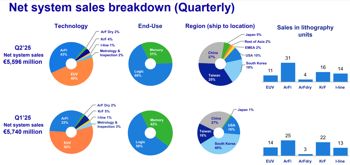
This portion of ASML revenue is at risk to some extent even if the relations between the two super powers seem to be stabilizing after a tough start of the year.
This is part of the reason of ASML’s sell-off over the last months as management was pretty cautious when it comes to guidance as they do not know what to expect, and guided for “between €44B & €60B by 2030” which is between no growth & 100% revenue increase or so for the next five years…
On the contrary, TSM is very confident in its future as its chips mostly go towards U.S. hardware manufacturers who then sell to China, avoiding direct transactions, and the market has rewarded the stock for it.
Financials.
Both companies have had a pretty rapid growth over the last decade or so with a clear acceleration over the last year as our world relies on their hardware more & more.

TSM growth is even more impressive as it starts from a higher volume which means a much higher growth in dollars, but both companies have accumulated more than 10% CAGR over the last 15 years which is really impressive and as I shared earlier, should not change as the future will rely on their hardware more - and TSM already shared that they expect a 15% - 20% CAGR for the next five years.
Both own a quasi monopoly on their respective areas, which means pricing power, a growing pricing power as demand is now higher than supply and those companies have to hike their prices to sell to the highest bidder only - this is mostly true for TSM lately as its production shifted to the U.S. ASML still has 52% of gross margins for 36% pre-tax margins for the last twelve months, which also highlights a really strong position on its market.

Those kinds of margins are the proof of a massive pricing power, and yield massive cash generation, which is where we will have a difference between both companies as their managements have a different style.
One will harvest cash in order to reinvest - into new fabs for example, while the other will redistribute to shareholders through both buybacks & dividends, a more western way of working.

In brief, both companies are pretty excellent at cash generation without much surprise and each has its own way of managing this cash generation.
Conclusion.
This is not the deepest technical review of both companies but it should be enough to give you a great overview of the technical aspects behind the actual frenzy on semiconductors - which has reasons to exist.
It should also give you a good overview of both ASML & TSM quasi monopolies and why they are so valuable & rewarded by the market. Both companies hold a crucial part of the manufacturing process of one of the most critical and demanded hardware of our time, without any signs of demand slowdown, on the contrary as we will need more compute in our smartphones, computers, cars & datacenters the next years to bring more AI use cases into the real world.
I personally intend to own both at a fair price, which is as usual shared on my weekly reviews & quarterly reports.
Many consider the AI revolution to be as important as the internet revolution. I would agree with them. And it will take years, decades & require massive amounts of compute to pursue this revoltion - combined with energy.

Compute starts with ASML & TSM, is optimized by companies like Nvidia & leveraged through different verticals, either through software like Meta or hardware like Tesla or Google’s autonomous vehicles. With much more to come.
But once again, it starts here, with ASML first & TSM second.